43

(b)
Split gap


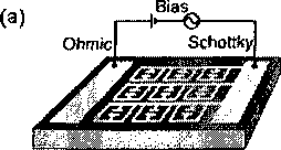
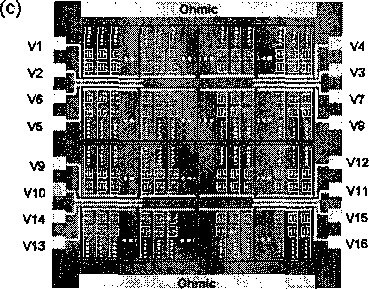
Figure 5.1 : (a) Each single pixel on the THz SLM contains a 4 × 4 mm2, ^2500
element array of metamaterial SRRs. These elements are connected together with
metal wires to serve as a metallic (Schottky) gate. An external voltage bias controls
the substrate charge carrier density near the split gaps, tuning the strength of the
resonance, (b) Diagram of the substrate and the depletion region near the split gap
of a single SRR, where the gray scale indicates the free charge carrier density, (c) The
THz SLM (not drawn to scale) is a 4 × 4 array of individual pixels in (a). Each pixel
is independently controlled by an external voltage between the 1 × 1 mm2 Schottky
electric pad and the ohmic contact.
Schottky electric pad and the ohmic contact. This device has low power dissipation,
drawing only a few milliamperes of current even when all the pixels are de-biased at
14 volts.
5.3 Experiments and results
Characterization of the THz SLM uses a THz time-domain spectroscopy system in
a transmission geometry with fiber-coupled photoconductive antennae for both THz
generation and detection. The linearly-polarized THz beam is collimated and directed
towards the modulator with the polarization of the THz electric field aligned along the
direction across the SRR split gaps. This setup is useful for evaluating the modulation
depth of each SLM pixel, the crosstalk between pixels, and the collective switching
More intriguing information
1. Income Mobility of Owners of Small Businesses when Boundaries between Occupations are Vague2. Death as a Fateful Moment? The Reflexive Individual and Scottish Funeral Practices
3. The name is absent
4. The name is absent
5. The name is absent
6. Assessing Economic Complexity with Input-Output Based Measures
7. Plasmid-Encoded Multidrug Resistance of Salmonella typhi and some Enteric Bacteria in and around Kolkata, India: A Preliminary Study
8. Road pricing and (re)location decisions households
9. A methodological approach in order to support decision-makers when defining Mobility and Transportation Politics
10. The name is absent