Vdd
Vdd
Vdd
Vdd
β∣MI
+
y∣∣δf∣∣
⅛4Γj≤fι ⅛
P
i,j pass transistors
threshold
current
segmentation
current


vi,j+1
Fig. 3. Schematics of a discontinuity unit.
output behavior (due to the boundedness of g) if the output
conductance R is large: Pii = 1, if the weighted measure
of the flow gradient and the brightness constraint deviation
is larger than a threshold a, and Pij = 0 otherwise.
Closing the feedback loop, the two relatively simple net-
work stages of the system solve a typical combinatorial
problem, which is computationally hard. Unlike in other
network solutions of such problems [6], the network ar-
chitecture is non-homogeneous. The discontinuity network
thereby performs a typical line process [8], although it re-
mains fully deterministic. Hence, the found solutions might
be only sub-optimal which can be reflected by hysteretic be-
havior in the activity of the discontinuity network.
3. HARDWARE AVLSI IMPLEMENTATION
An 11x11 array of the described optical flow system has
been implemented in a double-poly double-metal 0.8 m
BiCMOS process. Each pixel consists of an optical flow
unit plus two discontinuity units. The schematics of the op-
tical flow unit is basically as reported in [1] although im-
proved [7]. The estimated optical flow field is encoded as
the continuous voltage distributions Uij and Vij in two re-
sistive layers with respect to some reference potential, where
the output signal range is roughly ±0.5 V. The optical flow
units can reliably report the speed of visual motion over al-
most 3 orders of magnitude.
The schematics ofa single discontinuity unit are shown
in Figure 3. The circuit approximates the dynamics (4) with
the output Pij being inverted. The error measures (∣∣∆n∣∣
and ∣∣ΔF∣∣) are implemented by bump circuits [9] that pro-
vide the local segmentation current accordingly. The out-
put of the discontinuity units controls a pair of pass transis-
tors sitting in between two neighboring units of the optical
flow network in order to break the lateral conductances or
to leave them at some preset value .
In total, a single pixel consists of roughly 200 active el-
ements, occupying a chip area of (170 μm)2. A substantial
fraction of this area, however, is used for all the nearest-
neighbor connections of the different signals. The fill-factor
is at low 4% and power consumption is 80μWφixel in steady-
state.

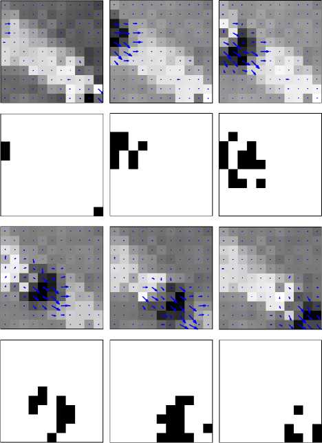
Fig. 4. Detecting motion discontinuities. The scanned se-
quence of the chip’s output while seeing a dark dot on a
light background, moving from the left upper to the right
lower corner of its visual field.
4. RESULTS
We waive a detailed characterization of the optical flow units
(which can be found in [7]) and report instead the response
of the complete system in two visual experiments, performed
under real-world conditions.
In the first example, the chip was presented with a stim-
ulus consisting of a dark moving dot on a light background.
Figure 4 shows the sampled responses of the chip while the
dot was moving from the upper left to the lower right cor-
ner of its visual field. The estimated optical flow field is
shown superimposed onto the images of the photorecep-
tor output, while the associated activity of the discontinu-
ity units (P and Q) is displayed as binary images below
each frame. Note that the activity pattern of the disconti-
nuity units approximately reflects the contour of the dark
dot. However, the chip has difficulties to achieve a closed
contour that completely separates figure and background.
Nevertheless, the optical flow estimate is improved insofar
as it predominantly preserves a sharp flow gradient at the
dot’s outline.
II - 334
More intriguing information
1. The name is absent2. Novelty and Reinforcement Learning in the Value System of Developmental Robots
3. Inflation and Inflation Uncertainty in the Euro Area
4. Migrant Business Networks and FDI
5. The name is absent
6. DIVERSITY OF RURAL PLACES - TEXAS
7. The name is absent
8. Behavior-Based Early Language Development on a Humanoid Robot
9. A Bayesian approach to analyze regional elasticities
10. Altruism and fairness in a public pension system