79
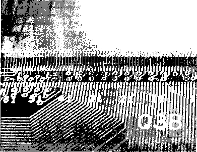
(a) Gold wires connecting SLM to PCB
ιιiιιιι
Γ ITTTlnr
J Я « » » S »
(b) Wire encapsulation
Figure B.11 : Microscope images of the wire-bonded SLM chip from VLSIP Technolo-
gies, Inc., showing the 1-mil gold wires between the die pads and the gold bond fingers
on the SLM board before and after encapsulating the wires with Hysol® FP4450.
100 mils. Cracks later observed on the attached SLM chips after wire-bonding bring
attention to the need for better chip protection (see Section 5.6).
B.6 Auxiliary components
The SLM control system uses a Mastech HY3005D-3 power supply to provide a 5V
input to the FPGA circuit and a 16V input to the line driver circuit. The maximum
current drawn from the 16V power supply is around 0.5A when all SLM pixels are
biased. The FPGA circuit receives a clock input from a Simpson 420 function gen-
erator. Monitored on a Tektronix TDS3054 digital oscilloscope, the system always
ensure synchronization between the pixel switching signals and the output trigger
signal to the Т-ray system. Always remember to set the oscilloscope as DC-coupled,
instead of AC-coupled, for proper operation.
Cables and connectors are purchased from Samtec, Inc. The control system the
More intriguing information
1. The name is absent2. The name is absent
3. The name is absent
4. The name is absent
5. Meat Slaughter and Processing Plants’ Traceability Levels Evidence From Iowa
6. Expectations, money, and the forecasting of inflation
7. The name is absent
8. The name is absent
9. The Triangular Relationship between the Commission, NRAs and National Courts Revisited
10. The name is absent