
Cable
sockets
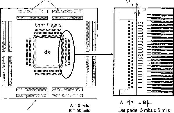
PCB board
C1 = 20 mils
C2 = 15mils
Bond fingers: 5 mils × 20 mils
78
Figure B. 10 : Detailed diagram near the square hole on the SLM board, with dimen-
sions of the PCB bond fingers, and of the bond pads (schottky and ohmic contacts)
of the SLM chip. Careful choices of the dimensions of bond pads and bond fingers,
and the distances among them ensure successful wire-bonding.
Due to the special requirements in this project, the company requires 5 additional
chips and boards for practice purpose. They successfully make all 1040 wire connec-
tions using the first practice chip, and subsequently bond all wires for the two SLM
chips, missing only one wire. Figure B. 11 displays some microscope images of the
wire bonds on one side of the chip.
For more information about the wire-bonding, contact Nicholas Moses from VL-
SIP Technologies, Inc.
Suggestion: The thicker the SLM board, the more external force it can withstand,
thus providing more protection of the attached SLM chip. Recommended thickness:
More intriguing information
1. Midwest prospects and the new economy2. The name is absent
3. Towards a framework for critical citizenship education
4. Spatial agglomeration and business groups: new evidence from Italian industrial districts
5. Mergers and the changing landscape of commercial banking (Part II)
6. Correlates of Alcoholic Blackout Experience
7. The name is absent
8. Existentialism: a Philosophy of Hope or Despair?
9. The name is absent
10. The name is absent