77

SUGGESTED FCB BONO FINGER LOCATIONS
(wires shown in red) ι..... ∖
These pads should
be squares
SiDE VIEW OF WIRE PRORLES
(a) SLM on PCB (side-view)
(b) Wire-bonding diagram
Figure B.9 : Diagrams of SLM board showing how the SLM chip is mounted and
wire-bonded onto the PCB (side-view (a) and top-view (b)).
dence in Figure B.8. The white silkscreen labels on the SLM board helps identify its
orientation and locate individual bond fingers (see Figure B.7).
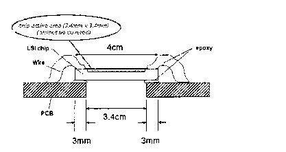
Figure B.9 and B. 10 are some diagrams sent to the wire-bonding company, VLSIP
Technologies, Inc., for their reference. The company first attaches the SLM chip
onto the PCB using Ablebond 84-3MV non-conductive epoxy on the 3mm-wide area
between the chip and the board (see Figure B.9(a)). This die attach epoxy can
withstand up to 425oC. Fixed on a 4.5” × 4.5” workholder with four 4-40 screws,
the KnS 1488L Turbo wire-bonding machine places 1.3-mil 99.99% pure gold wires
between each bond pad and PCB bond finger as in Figure B.9(b). The wire-bonding
temperatures is 150oC and the length of each bond wire must be in between 50 mils
and 150 mils, thus constraining the distance between the outer bond pads and outer
bond fingers. To protect the wire bonds, the final procedure fills up the gap between
the bond wires with a liquid encapsulant called Hysol® FP4450.
More intriguing information
1. The name is absent2. The fundamental determinants of financial integration in the European Union
3. The name is absent
4. MULTIPLE COMPARISONS WITH THE BEST: BAYESIAN PRECISION MEASURES OF EFFICIENCY RANKINGS
5. SAEA EDITOR'S REPORT, FEBRUARY 1988
6. Towards a framework for critical citizenship education
7. The name is absent
8. The problem of anglophone squint
9. Spousal Labor Market Effects from Government Health Insurance: Evidence from a Veterans Affairs Expansion
10. PRIORITIES IN THE CHANGING WORLD OF AGRICULTURE