76
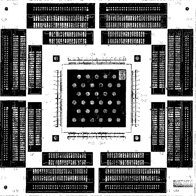
Figure В.8 : Screen capture of the top layer of the 4-layer SLM circuit board in
the Cadence PCB design software, showing partially the wire connections among the
various components. The middle upper layer is the ground plane, while the middle
lower layer is the power plane.
shorter than the 2”-transducer arm of the wire-bonding machine. The height of the
cable connectors are less than 6 mm so that they do not obstruct the transducer arm
during wire-bonding. Any on-board components need to be at least 1.25 mm from
the bond fingers.
The layout design procedures of the SLM board is the same as described in Sec-
tion B.4, using the Allegro Design Entry CIS schematics software and the Allegro
Cadence PCB layout software. See an example of the screen capture in Allegro Ca-
More intriguing information
1. Multimedia as a Cognitive Tool2. Short- and long-term experience in pulmonary vein segmental ostial ablation for paroxysmal atrial fibrillation*
3. The name is absent
4. The name is absent
5. The name is absent
6. Infrastructure Investment in Network Industries: The Role of Incentive Regulation and Regulatory Independence
7. ADJUSTMENT TO GLOBALISATION: A STUDY OF THE FOOTWEAR INDUSTRY IN EUROPE
8. The name is absent
9. The name is absent
10. The name is absent