72
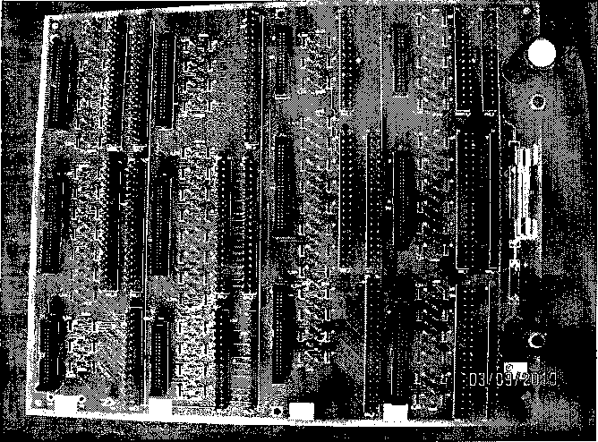
Figure В.4 : Line driver circuit board, which amplifies the voltage amplitudes of 512
FPGA control signals from 3V to 16V. The circuit board contains two banana cable
jacks, a Zener diode and a fuse for circuit protection, a bypass capacitor, connectors
to connect from the FPGA circuit and to the SLM board, and 512 voltage-amplifying
circuit made of bipolar transistors and resistors.
models the SLM pixel as a diode and the cables as inductors. Resistor values are
chosen to provide the correct voltage amplification and to draw reasonable current
from both the FPGA pins and the 16V power supply. The larger Rc is, the less
current drawn from the power supply but the switching becomes slower.
Here outlines the design procedure for the line driver circuit board.
1. Design the basic circuit model.
2. Determine all circuit components to use based on manufacturer, model, avail-
ability and packaging type.
3. Draw all component packages and the corresponding wire connections in the
More intriguing information
1. The name is absent2. The name is absent
3. The name is absent
4. Auctions in an outcome-based payment scheme to reward ecological services in agriculture – Conception, implementation and results
5. The name is absent
6. The name is absent
7. Does Competition Increase Economic Efficiency in Swedish County Councils?
8. The Veblen-Gerschenkron Effect of FDI in Mezzogiorno and East Germany
9. The name is absent
10. APPLICATIONS OF DUALITY THEORY TO AGRICULTURE