12
EURASIP Journal on Applied Signal Processing

-*-LMS
-о-CG, 5 iter.
FFT-based
DMI
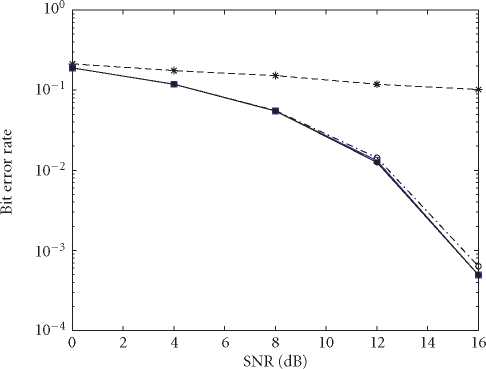
Figure 9: BER performance of 2 × 2 in Pedestrian-A channel; K = 14, G = 16, Lh = 3, T = 2, M = 2, and F = 10.

-*- LMS
—в— FFT-based
■ -O- CG, iter. = 5
→- DMI
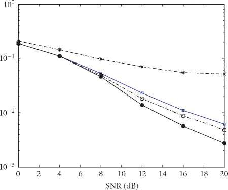
Figure 10: BER performance of 2 × 2 in Pedestrian-B channel; K = 14, G = 16, Lh = 6, T = 2, M = 2, and F = 10.
In Figure 13, we show the complexity trend for different J
and different LF versus the channel length for a (4 × 4) sys-
tem. Although the conjugate gradient algorithm has reduced
complexity compared with the DMI, the complexity reduc-
tion in the FFT-based algorithm is much more significant.
6. VLSI DESIGN ARCHITECTURE EXPLORATION
6.1. High-level-synthesis architecture scheduling
As a major revolution for the design of integrated circuits,
SoC architecture leads to a demand in new methodologies
and tools to address design, verification, and test problems in
this rapidly evolving area. There are many area/time/power
tradeoffs in the VLSI architectures. Extensive study of the
different architecture tradeoffs provides critical insights
into implementation issues and allows designers to identify
the critical performance bottlenecks in meeting real-time
requirements. Field-programmable gate array (FPGA) can
behave like a number of different ASICs with hardware
programmability to study architecture area/time tradeoffs.
This makes FPGA a good platform to build, verify, and
prototype SoC designs quickly. It has been well accepted as
a powerful rapid prototyping platform for the SoC architec-
tures in the literature [13, 25]. A detailed discussion on the
tradeoffs using FPGA and DSP for real-time implementation
More intriguing information
1. Distortions in a multi-level co-financing system: the case of the agri-environmental programme of Saxony-Anhalt2. fMRI Investigation of Cortical and Subcortical Networks in the Learning of Abstract and Effector-Specific Representations of Motor Sequences
3. The problem of anglophone squint
4. Who is missing from higher education?
5. El Mercosur y la integración económica global
6. The name is absent
7. Multiple Arrhythmogenic Substrate for Tachycardia in a
8. The Impact of Cognitive versus Affective Aspects on Consumer Usage of Financial Service Delivery Channels
9. The name is absent
10. The changing face of Chicago: demographic trends in the 1990s