Yuanbin Guo et al.
15

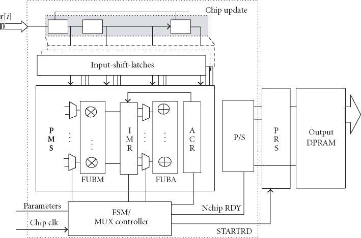
Figure 15: Throughput mode correlation update module using PMS.
design flow. In most cases, the manual tradeoff study of a
complex design with hundreds of multipliers could be ex-
tremely time consuming and difficult. However, we can al-
most achieve the most efficient design architecture for a given
specification using the architecture scheduling in Catapult C,
especially for the computation-intensive algorithms. Com-
pared with the conventional hand-code and schematic-based
design methodologies, the Catapult C-based methodology
demonstrates not only improved productivity, but also a ca-
pability to study the architecture tradeoffs extensively in a
short design cycle.
6.2. Real-time VLSI architecture exploration
The complete equalizer includes two major steps: the com-
putation of the equalizer coefficients w and the actual FIR
filtering using the updated equalizer taps as in wHrA(i). The
update of the equalizer coefficients is a block-based opera-
tion depending on the channel varying speed. The FIR filter-
ing depends on the chip rate. Thus, we need to compute the
L-tap convolution for each input chip from the N receive an-
tennas for the FIR filtering within fclk/ fchip cycles, where fclk
and fchip are the system clock rate and chip rate, respectively.
The WCDMA chip rate is 3.84 MHz. We applied a clock rate
of 38.4 MHz for the Xilinx Virtex-II V6000-4 FPGA. There
will be 10 cycles time constraint per input chip. For the tap
solver, the experiment shows that 2 updates per slot are suf-
ficient to provide acceptable performance for slow and me-
dian fading channels. Since there are 1920 chips per slot, the
latency requirement for each update is 250 microseconds.
We schedule architectures in two basic modes according
to the real-time behavior of the subsystem in Catapult C: the
throughput mode or the block mode. Throughput mode as-
sumes that there is a top-level main loop for each incoming
sample, which is processed immediately in the computation
period. The module processes for each input sample period-
ically, so there is a strict limit for the processing time. Block-
mode processes once after a block data is ready. Because
the finite-state machine (FSM) usually depends on complex
logic and extensive memory access, the computation patten
is more like a processor architecture in loading data to the
functional units. In the following, we use two typical design
modules to demonstrate these different working modes.
6.2.1. Scalable pipelined-multiplexing scheduler
The covariance estimation is computed as
1 NB-1
Rrr = N^-J Σ rA(i)rH(i) (31)
assuming ergodicity. Theoretically, the front-end covariance
estimation module can also be designed in block mode sim-
ilar to a processor implementation. However, this architec-
ture causes a large processing latency and requires big ping
pong buffers to store the input samples. For NB = 960 chips
per block, the fastest RTL takes more than 6 millisecond la-
tency because the heavy memory access stalls the pipelining
and does not provide sufficient parallelism. To meet the real-
time requirement, a scalable architecture is designed with
throughput mode as in Figure 15. L input-shift-latches (ISLs)
shift the new samples and the delayed samples in one cycle.
The core is the pipelined-multiplexing scheduler (PMS) with
a set of functional-unit banks (FUB) for both multipliers
and adders. The temporary values are stored in intermediate-
multiplication registers (IMRs) and accumulation-register
More intriguing information
1. The name is absent2. Economic Evaluation of Positron Emission Tomography (PET) in Non Small Cell Lung Cancer (NSCLC), CHERE Working Paper 2007/6
3. A Unified Model For Developmental Robotics
4. Delivering job search services in rural labour markets: the role of ICT
5. Markets for Influence
6. The Prohibition of the Proposed Springer-ProSiebenSat.1-Merger: How much Economics in German Merger Control?
7. The name is absent
8. Standards behaviours face to innovation of the entrepreneurships of Beira Interior
9. Spatial agglomeration and business groups: new evidence from Italian industrial districts
10. Credit Market Competition and Capital Regulation